| CPC G06F 9/30047 (2013.01) [G06F 9/30018 (2013.01); G06F 9/30036 (2013.01); G06F 9/30043 (2013.01); G06F 9/30105 (2013.01); G06F 9/3016 (2013.01); G06F 9/3824 (2013.01); G06F 9/3836 (2013.01); G06F 12/0897 (2013.01)] | 17 Claims |
|
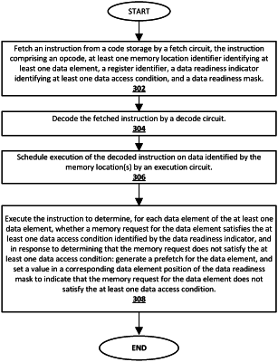
1. A method comprising:
decoding a single instruction by a decode circuit, the single instruction comprising an opcode, at least one source memory location identifier, a destination register identifier, a data readiness indicator identifying at least one data access condition, and a data readiness mask; and
executing the decoded instruction by an execution circuit by:
for each data element of the identified source memory location,
determining whether the data access condition for that data element is satisfied, and
in response to determining that the data access condition for the data element is not satisfied:
generating a prefetch request for the data element,
setting a value in a corresponding data element position of the identified destination register, and
setting a masked value in a corresponding data element position of the data readiness mask.
|