| CPC G06F 3/0659 (2013.01) [G06F 3/0604 (2013.01); G06F 3/0673 (2013.01); H01L 25/0652 (2013.01); H01L 25/18 (2013.01)] | 20 Claims |
|
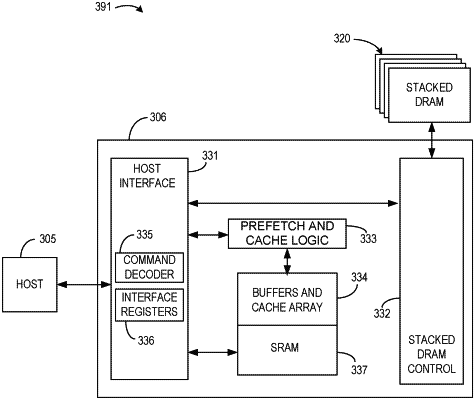
1. A logic die for a storage device, the logic die comprising:
a first interface to communicate with a stack of memory die of the storage device;
a second interface configured to couple with a host device;
a second memory accessible from the second interface; and
processing circuitry configured to:
initiate a first operation for the stack of memory die in response to a first request from the host device, wherein the first request uses a first command/address bus of the second interface to identify the first operation;
initiate a second operation for the stack of memory die in response to a second request from the host device, wherein the second request uses a second command/address bus of the second interface to identify the second operation as a read operation or a write operation; and
initiate a third operation for the second memory in response to a third request from the host device, wherein the third request uses both the first command/address bus and the second command/address bus to identify the third operation for the second memory.
|