| CPC G06F 3/0448 (2019.05) [H01H 13/48 (2013.01)] | 14 Claims |
|
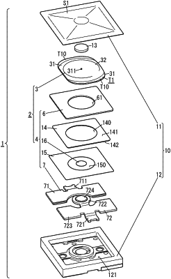
1. An input device, comprising:
a fixed electrode;
a movable electrode having a plate shape, the movable electrode having a hole penetrating its central part in a thickness direction thereof; and
a movable member configured to elastically deform by receiving pressing force to relatively displace the movable electrode toward the fixed electrode, wherein:
the movable member includes a summit part configured to pass through the hole of the movable electrode and approach a part of the fixed electrode, when the movable member is elastically deformed by receiving the pressing force, and
the movable member includes an outer peripheral part, and the outer peripheral part includes a suppression structure configured to suppress the movable member from being elastically deformed by the pressing force.
|