| CPC G06F 3/0445 (2019.05) [G06F 3/0446 (2019.05); H01L 27/124 (2013.01); H01L 27/1259 (2013.01); G06F 2203/04103 (2013.01)] | 13 Claims |
|
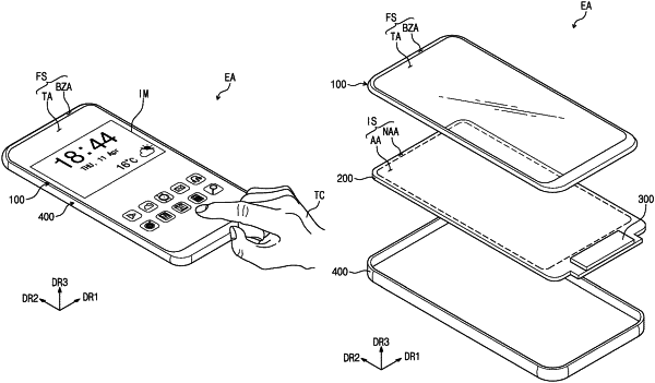
1. An electronic apparatus, comprising:
a display unit; and
an input sensing unit on the display unit,
wherein:
the display unit comprises insulating layers, a signal line, a pad connected to an end portion of the signal line, and circuit elements; and
the insulating layers comprise a first insulating layer covering the circuit elements and exposing at least a portion of the circuit elements,
wherein the input sensing unit comprises:
a first conductive layer;
a second conductive layer including sensing patterns; and
a second insulating layer between the first conductive layer and the second conductive layer, the second insulating layer exposing at least a portion of the first conductive layer, and
wherein:
the display unit further comprises a first electrode, a second electrode, and a light emitting layer between the first and second electrodes;
the first insulating layer and the second insulating layer are disposed between the end portion of the signal line and the pad;
an insulating layer between the end portion of the signal line and the pad is defined as a pad insulating layer; and
a maximum thickness of the pad insulating layer is greater than a sum of a thickness of the first insulating layer and a thickness of the second insulating layer in an area overlapping the signal line.
|