| CPC G03F 1/24 (2013.01) [B23K 26/06 (2013.01); H01L 21/268 (2013.01)] | 18 Claims |
|
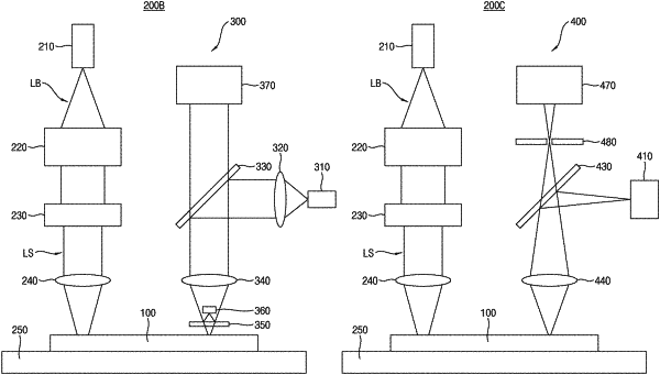
1. A laser annealing method performed on a reflective photomask, the laser annealing method comprising:
preparing a reflective photomask including a pattern area and a border area surrounding the pattern area; and
irradiating a laser beam onto the border area of the reflective photomask,
wherein the laser beam has a pulse shape,
irradiating of the laser beam comprises split-irradiating a plurality of laser beam spots onto the border area,
each of the plurality of laser beam spots is shaped using a beam shaper, and
an energy level of an edge portion of each of the plurality of laser beam spots is lower than that of a center portion of each of the plurality of laser beam spots.
|