| CPC G01T 1/17 (2013.01) [G01T 1/247 (2013.01)] | 6 Claims |
|
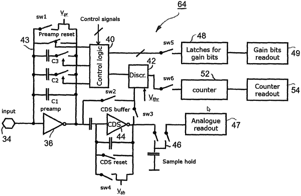
1. A dual mode detector system for photon detection that is configured for operation either in single photon counting mode or in charge integrating mode with or without gain switching, the detector system comprising:
a) a layer of photosensitive material;
b) an N×M array of photo-detector diodes arranged in said layer of photosensitive material, each of said photo-detector diodes having a bias potential interface connected to a bias potential and a diode output interface;
c) a N×M array of high gain, low noise readout unit cells, one readout unit cell for each photo-detector diode; and
d) each of said readout unit cells having:
d1) an input interface connecting said diode output interface to a high-gain charge-to-voltage amplifier;
d2) said high-gain charge-to-voltage amplifier having a feedback network between input and output with:
d21) a number of feedback capacitors which can be switched in or out from said feedback network;
d22) a fixed or controllable feedback resistance, using a preamp voltage, which can be switched in or out from said feedback network, as required in the single photon counting mode; and
d23) a preamp reset switch configured to reset a voltage between terminals of said feedback capacitors to zero in the charge integrating mode;
d3) said high-gain charge-to-voltage amplifier being connected to a shaper/CDS having a feedback network between input and output, said shaper being configured to amplify and reduce a noise content of a signal coming from a preamplifier in the photon counting mode, and to act as a correlated double sampling stage in the charge integrating mode;
d4) said shaper having a feedback network between input and output, with:
d41) a number of feedback capacitors which can be switched in or out from said feedback network;
d42) a fixed or controllable feedback resistance, needed in single photon counting mode, using a shaper voltage, which can be switched in or out from the feedback network;
d43) a CDS reset switch, needed to reset a voltage between the terminal of said feedback capacitors to a voltage of zero in the charge integrating mode;
d5) a discriminator receiving as an input an output voltage of the high-gain charge-to-voltage amplifier in the charge integrating mode and the output of the shaper in the single photon counting mode, thus detecting when the preamplifier reaches saturation in the charge integrating mode or when a photon was impinging on said photo detector diode in the single photon counting mode;
d6) a counter connected to said discriminator in the single photon counting mode, needed to count the number of photons;
d7) a number of switches, said switches being controlled to enable a use of said high-gain charge-to-voltage amplifier, said shaper and said discriminator in both modes;
d8) a control logic, connected to the output of said discriminator and to control signals coming from a chip periphery, generating necessary steering signals for a preamplifier feedback network;
d9) a counter readout having a required digital circuitry configured to read out said counter;
d10) a gain bit readout having required digital circuitry to read out the latches for the gain bits; and
d11) an analog readout having required analog circuitry needed to read out a voltage of a sample-and-hold circuit; and
e) a channel readout architecture formed of:
e1) one or more analog multiplexers connected to the analog readout circuitry of all channels and configured to, according to a channel selection and MUX control signals, route selected channels to one or more analog outputs;
e2) one or more digital multiplexers connected to the counter readout circuitry of all channels and configured to, according to a channel selection and MUX control signals, route selected channels to one or more digital outputs; and
e3) one or more digital multiplexers connected to the gain bit readout circuitry of all channels and configured to, according to a channel selection and MUX control signals, route a selected channels to one or more digital outputs.
|