| CPC G01R 31/3177 (2013.01) [G01R 31/31718 (2013.01); G01R 31/31724 (2013.01); G06F 11/1048 (2013.01); G06F 11/1068 (2013.01); G11C 29/36 (2013.01); G11C 29/42 (2013.01); G11C 29/56004 (2013.01); G11C 2029/3602 (2013.01); G11C 2029/5602 (2013.01)] | 20 Claims |
|
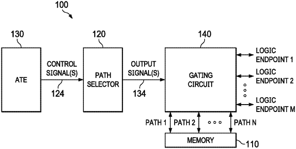
19. A method, comprising:
receiving a control signal to control data access to data paths that are operatively coupled between memory and an external device;
generating an output signal that indicates a selected data path in response to the control signal;
enabling at least one clock gate in a gating circuit to control the selected data path are to be accessed by the external device in response to the output signal, wherein the gating circuit comprises a first set of logic gates, a second set of logic gates, and a decoder, wherein an output of the first set of the logic gates is coupled to an input of the decoder, wherein an output of the decoder are coupled to an input of the second set of logic gates, wherein an output of the second set of logic gates is operatively coupled to the memory; and
accessing the memory, by the external device, via the selected data path enabled by the enabling.
|