US 11,933,843 B2
Techniques to enable integrated circuit debug across low power states
Keith A. Jones, Forest Grove, OR (US); Wai Mun Ng, Bukit Mertajam (MY); Thomas A. Lyda, Folsom, CA (US); Subinlal Pk, Kozhikode (IN); Sankaran Menon, Austin, TX (US); Vui Yong Liew, Bukit Mertajam (MY); and Kristan K. Wiseley, Folsom, CA (US)
Assigned to Intel Corporation, Santa Clara, CA (US)
Filed by Intel Corporation, Santa Clara, CA (US)
Filed on Jul. 15, 2021, as Appl. No. 17/377,264.
Claims priority of provisional application 63/053,421, filed on Jul. 17, 2020.
Claims priority of application No. 202041030496 (IN), filed on Jul. 17, 2020; and application No. PI2020003707 (MY), filed on Jul. 17, 2020.
Prior Publication US 2022/0018901 A1, Jan. 20, 2022
Int. Cl. G01R 31/317 (2006.01); G01R 31/3183 (2006.01); G01R 31/3185 (2006.01)
CPC G01R 31/31721 (2013.01) [G01R 31/31705 (2013.01); G01R 31/318314 (2013.01); G01R 31/318533 (2013.01)] 24 Claims
OG exemplary drawing
 
1. An integrated circuit, comprising:
a plurality of circuit blocks; and
a control circuit coupled to the plurality of circuit blocks, the control circuit to:
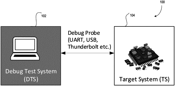
identify a probe type of a probe that connects the integrated circuit to a debug test system;
identify a debug use case to be used by the debug test system; and
turn off or disable at least one of a clock or a power to one or more circuit blocks of the plurality of circuit blocks which are not associated with the probe type and the debug use case.