| CPC G01R 31/31701 (2013.01) [G01R 31/31713 (2013.01); G01R 31/31721 (2013.01); G01R 31/31724 (2013.01); G01R 31/3183 (2013.01)] | 13 Claims |
|
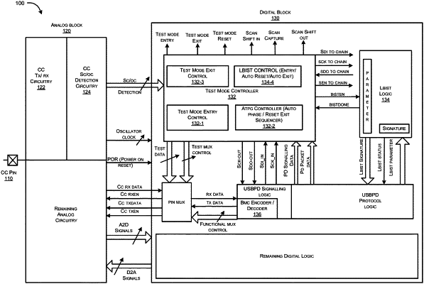
1. A system for facilitating design for testing (DFT) architecture for use in testing an integrated circuits (IC) associated with universal serial bus power delivery (USBPD) using a single input-output (I/O) pin, the system comprising:
an analog block comprising a USBPD configuration channel (CC) circuitry that detects short circuit (SC) and over currents (OC) on a CC pin, receives and transmits data on the CC pin for a USBPD framework;
a digital block comprising a USBPD block handling USBPD communication packets and signalling; and
a test mode controller configured to receive CC pin input/output (I/O) data, SC detection, and OC detection, as well as test related USBPD packet and signalling data from the USBPD block,
wherein the test mode controller is configured to detect or activate a test mode based on a USB PD packet data and USB PD signalling data received on the CC pin, wherein the test mode controller is configured to control the test mode with respect to the DFT architecture,
wherein the test modes includes an analog test mode comprising trims and observation modes, and a digital test mode comprising logic built-in self-test (LBIST) mode for covering and detecting defects in digital components associated with integrated circuits, an automatic test pattern generation (ATPG) mode operating at lower speeds which is directed to covering and further detecting the defects that are uncovered or undetected by the LBIST mode and digital observation modes for debug purposes,
wherein the analog and digital test modes are implemented with respect to the single I/O pin which is the CC pin with respect to USBPD integrated circuits, and
wherein the ATPG test mode operates based on a scan chain technique that includes a sequential shift-in phase and shift-out phase, with the CC pin corresponding to input and output respectively during shift-in and shift-out operation.
|