| CPC G01N 27/228 (2013.01) [G01N 33/02 (2013.01); H01Q 1/38 (2013.01); H01Q 7/00 (2013.01); H05K 1/092 (2013.01); H05K 1/16 (2013.01); H05K 2201/10098 (2013.01)] | 39 Claims |
|
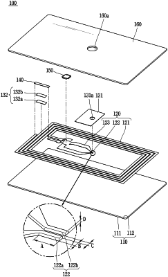
1. A sensor comprising:
a substrate;
an antenna pattern formed in a spiral shape on the substrate;
a first electrode and a second electrode formed on the substrate and spaced apart from each other in parallel;
a circuit wiring formed to be connected to each of the first electrode and the second electrode;
an element bonded to the antenna pattern and the circuit wiring; and
a circuit insulating layer disposed on at least a portion of the circuit wiring and having a window to expose the first electrode and the second electrode,
wherein cross sections of the first electrode and the second electrode each has a curvature.
|