| CPC B81C 1/00238 (2013.01) [B81B 7/008 (2013.01); B81C 1/00333 (2013.01); H01L 24/09 (2013.01); H01L 24/89 (2013.01); B81B 2207/07 (2013.01); B81C 2201/0132 (2013.01); B81C 2203/0109 (2013.01); B81C 2203/0785 (2013.01); B81C 2203/0792 (2013.01); H01L 2224/091 (2013.01); H01L 2224/80013 (2013.01); H01L 2224/80895 (2013.01)] | 20 Claims |
|
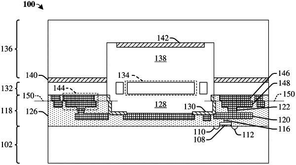
1. A microelectromechanical system (MEMS) device, comprising:
a metallization structure disposed over a first semiconductor substrate, wherein the metallization structure comprises a plurality of conductive features embedded in a dielectric structure, wherein the dielectric structure has a first portion disposed over a second portion, and wherein a first sidewall of the first portion of the dielectric structure is laterally spaced from a first sidewall of the second portion of the dielectric structure;
a cavity disposed in the metallization structure, wherein the cavity is disposed laterally between the first sidewall of the first portion of the dielectric structure and a second sidewall of the first portion of the dielectric structure opposite the first sidewall of the first portion of the dielectric structure; and
a second semiconductor substrate disposed over the metallization structure, wherein the second semiconductor substrate comprises a movable element disposed within the cavity.
|