US 12,255,047 B1
Embedded high-z marker material and process for alignment of multilevel ebeam lithography
Christopher Bohn, Santa Monica, CA (US); Maxwell Choi, Thousand Oaks, CA (US); Melanie Yajima, Los Angeles, CA (US); Sieu Ha, Los Angeles, CA (US); Maggy Lau, Stevenson, CA (US); Clayton Jackson, Los Angeles, CA (US); Wonill Ha, Thousand Oaks, CA (US); and Matthew Borselli, Calabasas, CA (US)
Assigned to HRL LABORATORIES, LLC, Malibu, CA (US)
Filed by HRL LABORATORIES, LLC, Malibu, CA (US)
Filed on Oct. 10, 2023, as Appl. No. 18/484,348.
Application 18/484,348 is a division of application No. 17/121,109, filed on Dec. 14, 2020, granted, now 11,823,864.
Claims priority of provisional application 63/007,104, filed on Apr. 8, 2020.
Int. Cl. H01J 37/317 (2006.01); G03F 9/00 (2006.01); H01L 21/033 (2006.01); H01L 23/544 (2006.01)
CPC H01J 37/3177 (2013.01) [G03F 9/7076 (2013.01); G03F 9/708 (2013.01); G03F 9/7088 (2013.01); H01L 21/0332 (2013.01); H01L 21/0337 (2013.01); H01L 23/544 (2013.01); H01J 2237/24475 (2013.01); H01J 2237/334 (2013.01); H01L 2223/54426 (2013.01)] 4 Claims
OG exemplary drawing
 
1. A semiconductor device comprising:
a substrate;
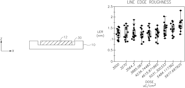
an alignment marker embedded in the substrate, the alignment marker comprising tantalum (Ta) and having a line edge roughness of less than 2.5 nm;
a plurality of transistors in the substrate; and
a plurality of metal interconnects and metal vias connected to the plurality of transistors.