| CPC H10N 60/0912 (2023.02) [B82Y 10/00 (2013.01); H01L 21/2855 (2013.01); H01L 21/76877 (2013.01); H01L 21/76891 (2013.01); H10N 60/01 (2023.02); H10N 60/0156 (2023.02); H10N 60/10 (2023.02); H10N 60/12 (2023.02); H10N 60/805 (2023.02); H10N 60/855 (2023.02); H10N 69/00 (2023.02); G06N 10/00 (2019.01)] | 12 Claims |
|
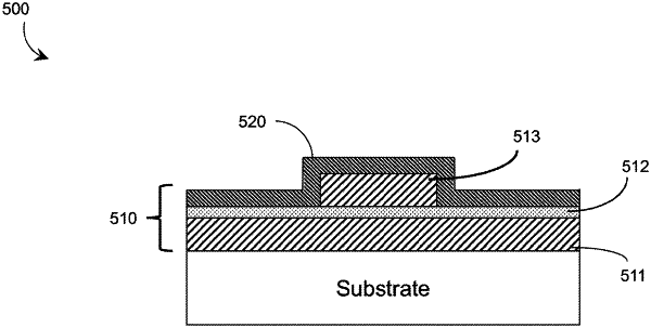
1. A method of fabricating a superconducting integrated circuit, the method comprising:
depositing a first dielectric layer;
depositing a negative photoresist mask over the first dielectric layer that traces out a negative pattern of a desired circuit pattern such that the desired circuit pattern corresponds to regions of the first dielectric layer that are not directly covered by the negative photoresist mask;
etching the desired circuit pattern into the first dielectric layer to produce open features in the first dielectric layer;
depositing a first superconducting metal layer over the first dielectric layer to at least partially fill the open features in the first dielectric layer;
planarizing the first superconducting metal layer;
depositing a second dielectric layer to produce a desired inner layer dielectric thickness, wherein the inner layer dielectric thickness is controlled by a deposition process; and
depositing a second superconducting metal layer above the second dielectric layer.
|