| CPC H10N 52/80 (2023.02) [G11C 11/161 (2013.01); G11C 11/1673 (2013.01); G11C 11/1675 (2013.01); G11C 11/18 (2013.01); G11C 11/22 (2013.01); H10B 61/00 (2023.02); H10N 52/00 (2023.02); G11C 11/1659 (2013.01)] | 19 Claims |
|
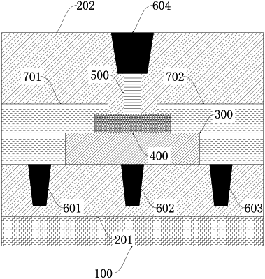
1. A magnetic random access storage unit, comprising:
a semiconductor substrate;
a first insulating medium layer formed on the semiconductor substrate;
a ferroelectric thin film layer disposed on the first insulating medium layer;
a bottom electrode formed on the ferroelectric thin film layer;
a tunnel junction formed on the bottom electrode;
a first metal interconnection portion connected to a first end of the bottom electrode;
a second metal interconnection portion connected to the ferroelectric thin film layer;
a third metal interconnection portion connected to a second end of the bottom electrode, the second end and the first end being respectively located on both sides of the bottom electrode;
a fourth metal interconnection portion connected to the tunnel junction;
a first interconnection metal layer formed on the first insulating medium layer; the first interconnection metal layer being used for the connection of the first metal interconnection portion to the first end of the bottom electrode;
a second interconnection metal layer formed on the first insulating medium layer, the second interconnection metal layer being used for the connection of the third metal interconnection portion to the second end of the bottom electrode;
a second insulating medium layer formed on the first interconnection metal layer and the second interconnection metal layer, the tunnel junction being disposed in the second insulating medium layer; and
a fourth via disposed on the tunnel junction and formed in the second insulating medium layer, the fourth metal interconnection portion being formed in the fourth via.
|