| CPC H10K 59/65 (2023.02) [G02B 7/021 (2013.01); H04B 1/3827 (2013.01); H04N 23/51 (2023.01); H10K 50/84 (2023.02); H10K 50/86 (2023.02); H10K 50/87 (2023.02); H10K 59/12 (2023.02); H10K 59/40 (2023.02); H01L 27/14623 (2013.01); H01L 27/14627 (2013.01)] | 17 Claims |
|
1. An electronic device comprising:
a housing;
a display disposed in an internal space of the housing to be viewable from an outside and including a display area; and
a camera module disposed under the display overlapping at least a part of the display area and not including an aperture structure,
wherein the camera module includes:
a lens housing;
a plurality of lenses disposed on the lens housing; and
an image sensor disposed under the plurality of lenses,
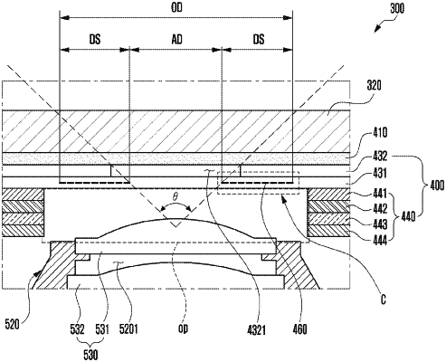
wherein the display includes:
a display panel; and
a light blocking member disposed inside of the display panel, the light blocking member comprising light blocking material and a light transmission region surrounded at least partially by the light blocking material,
wherein the light transmission region overlaps at least parts of the plurality of lenses when the display is viewed from above,
wherein the display panel comprises:
a substrate layer;
an intermediate layer including a plurality of pixel electrodes laminated on an upper portion of the substrate layer, organic light-emitting layers disposed on the plurality of pixel electrodes, respectively, and an opposite electrode disposed on upper portions of the organic light-emitting layers; and
an encapsulation layer disposed on an upper portion of the intermediate layer, wherein the light blocking member is disposed at the intermediate layer.
|