| CPC H10K 59/353 (2023.02) [H10K 50/865 (2023.02); H10K 59/1213 (2023.02); H10K 71/00 (2023.02); H10K 59/1201 (2023.02)] | 20 Claims |
|
1. An array substrate, comprising:
a substrate comprising a plurality of sub-pixel regions and a plurality of monochromatic light-emitting regions;
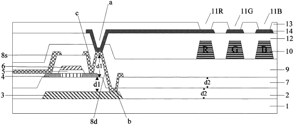
a thin film transistor located in each of the sub-pixel regions on the substrate, and the thin film transistor comprises a gate, an active layer, and a source-drain electrode;
a passivation layer located on a side, away from the substrate, of the thin film transistor;
a color resist located on a side, away from the substrate, of the passivation layer and located in the monochromatic light-emitting regions;
a planarization layer located on a side, away from the substrate, of the color resist and the passivation layer;
an anode located on a side, away from the substrate, of the planarization layer and electrically connected to a drain electrode in the source-drain electrode through a first through hole penetrating through the passivation layer and the planarization layer; and
dielectric layers located between the source-drain electrode and the substrate, wherein a thickness of at least one of the dielectric layers between the first through hole and the substrate is greater than a thickness of the at least one of the dielectric layers between the color resist and the substrate;
wherein the dielectric layers comprise: a buffer layer located between the substrate and the thin film transistor, and a thickness of the buffer layer between the thin film transistor and the substrate is greater than a thickness of the buffer layer between the color resist and the substrate.
|