| CPC H10K 59/1315 (2023.02) [H10K 59/126 (2023.02); H10K 59/38 (2023.02); H10K 71/00 (2023.02); H10K 59/1201 (2023.02)] | 16 Claims |

|
1. A display panel, wherein the display panel comprises:
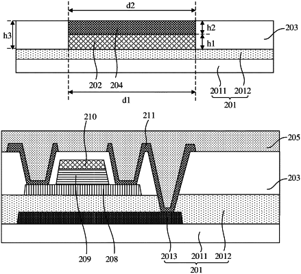
a substrate, wherein the substrate is divided into a plurality of sub-pixel regions and a pixel separating region located between two neighboring columns of the sub-pixel regions;
a resistance reducing trace, wherein the resistance reducing trace is provided on the pixel separating region of the substrate;
an inter-layer-medium layer, wherein the inter-layer-medium layer is provided on the substrate, and the inter-layer-medium layer has an opening exposing the resistance reducing trace; and
a signal line, wherein the signal line is provided within the opening, the signal line is connected to the resistance reducing trace, the signal line is distributed in a column direction along the display panel, and in a row direction along the display panel, a width of the opening is greater than or equal to a width of the signal line.
|