| CPC H10K 59/131 (2023.02) [G06F 3/0412 (2013.01); H10K 50/844 (2023.02); H10K 59/121 (2023.02); H10K 59/122 (2023.02); H10K 59/40 (2023.02); H10K 59/65 (2023.02); H10K 77/111 (2023.02); G06F 3/0445 (2019.05); G06F 3/0446 (2019.05); H10K 2102/311 (2023.02)] | 19 Claims |
|
1. A display panel, comprising a base substrate, a plurality of pixel drive circuit units, and n first signal lines,
wherein the display panel further comprises a light emitting element, the light emitting element comprises a first electrode, a light emitting layer, and a second electrode, the first electrode is on a side of the n first signal lines away from the base substrate, and is electrically connected with at least one pixel drive circuit unit of the plurality of pixel drive circuit units, the second electrode is on a side of the first electrode away from the base substrate, the light emitting layer is between the first electrode and the second electrode, and the light emitting element comprises one type among a red light emitting element, a green light emitting element, and a blue light emitting element;
the base substrate comprises a light-transmitting region, a display region at least partially surrounding the light-transmitting region, and a peripheral region between the display region and the light-transmitting region;
the plurality of pixel drive circuit units are at least partially in the display region;
the n first signal lines are configured to supply a first signal to the plurality of pixel drive circuit units;
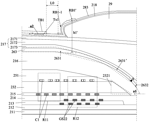
at least one of the n first signal lines comprises a first main body portion located in the display region, a first extending portion and a first bending portion located in the peripheral region, the first extending portion is electrically connected with the first main body portion, and the first bending portion at least partially surrounds the light-transmitting region, and is farther away from the first main body portion than the first extending portion;
among the n first signal lines, a distance between first extending portions of two adjacent first signal lines is greater than a distance between first bending portions of the two adjacent first signal lines; and
at least one of the plurality of pixel drive circuit units comprises a low temperature polysilicon thin film transistor and an oxide transistor;
the display panel further comprises: a first insulating layer, a second insulating layer, a third insulating layer, and a fourth insulating layer arranged in a direction away from the base substrate,
wherein the plurality of pixel drive circuit units each comprise a low temperature polysilicon thin film transistor and an oxide transistor, one of the low temperature polysilicon thin film transistor and the oxide transistor is electrically connected with the light emitting element, and the light emitting element is on a side of the fourth insulating layer away from the base substrate;
the second electrode comprises a first sub-portion and a second sub-portion in the peripheral region, an orthogonal projection of the first sub-portion on the base substrate at least partially overlaps with an orthogonal projection of the fourth insulating layer on the base substrate, an orthogonal projection of the second sub-portion on the base substrate does not overlap with the orthogonal projection of the fourth insulating layer on the base substrate;
an orthogonal projection overlap area between the first sub-portion and first extending portions of the n first signal lines on the base substrate is S3, an orthogonal projection overlap area between the second sub-portion and first bending portions of the n first signal lines on the base substrate is S4, and
S3>S4.
|
|
19. A display panel, comprising a base substrate, a plurality of pixel drive circuit units, and n first signal lines,
wherein the display panel further comprises a light emitting element, the light emitting element comprises a first electrode, a light emitting layer, and a second electrode, the first electrode is on a side of the n first signal lines away from the base substrate, and is electrically connected with at least one pixel drive circuit unit of the plurality of pixel drive circuit units, the second electrode is on a side of the first electrode away from the base substrate, the light emitting layer is between the first electrode and the second electrode, and the light emitting element comprises one type among a red light emitting element, a green light emitting element, and a blue light emitting element,
wherein the base substrate comprises a light-transmitting region, a display region at least partially surrounding the light-transmitting region, and a peripheral region between the display region and the light-transmitting region;
the plurality of pixel drive circuit units are at least partially in the display region;
the n first signal lines are configured to supply a first signal to the plurality of pixel drive circuit units;
at least one of the n first signal lines comprises a first main body portion located in the display region, a first extending portion and a first bending portion located in the peripheral region, the first extending portion is electrically connected with the first main body portion, and the first bending portion at least partially surrounds the light-transmitting region, and is farther away from the first main body portion than the first extending portion;
among the n first signal lines, a distance between first extending portions of two adjacent first signal lines is greater than a distance between first bending portions of the two adjacent first signal lines; and
the plurality of pixel drive circuit units each only comprise a low temperature polysilicon thin film transistor;
the display panel further comprises: a first insulating layer, a second insulating layer, a third insulating layer, and a fourth insulating layer arranged in a direction away from the base substrate,
wherein the plurality of pixel drive circuit units each comprise the low temperature polysilicon thin film transistor, the low temperature polysilicon thin film transistor is electrically connected with the light emitting element, and the light emitting element is on a side of the fourth insulating layer away from the base substrate;
the second electrode comprises a first sub-portion and a second sub-portion in the peripheral region, an orthogonal projection of the first sub-portion on the base substrate at least partially overlaps with an orthogonal projection of the fourth insulating layer on the base substrate, an orthogonal projection of the second sub-portion on the base substrate does not overlap with the orthogonal projection of the fourth insulating layer on the base substrate;
an orthogonal projection overlap area between the first sub-portion and first extending portions of the n first signal lines on the base substrate is S3, an orthogonal projection overlap area between the second sub-portion and first bending portions of the n first signal lines on the base substrate is S4, and
S3>S4.
|