| CPC H10K 59/131 (2023.02) [H10K 59/1201 (2023.02); H10K 59/124 (2023.02); H10K 71/162 (2023.02)] | 19 Claims |
|
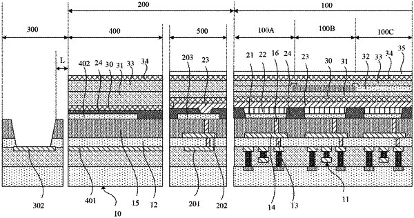
1. A display substrate, comprising:
a silicon-based substrate having a display area, a binding area located on one side of the display area, and a trace area located between the display area and the binding area;
a trace protection structure being arranged on the silicon-based substrate in the trace area, and a pad assembly being integrated in the silicon-based substrate in the binding area; and a minimum distance between an edge of an orthographic projection of the trace protection structure on the silicon-based substrate and an edge of an orthographic projection of an opening of the pad assembly on the silicon-based substrate being smaller than a maximum size of one subpixel.
|