| CPC H10K 59/131 (2023.02) | 19 Claims |
|
1. A display panel comprising:
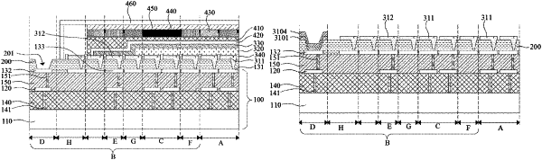
a drive backplane comprising a driving circuit layer, a metal wiring layer, a first insulating layer and a reflective electrode layer sequentially laminated; wherein the first insulating layer has a plurality of first via holes, and each of the plurality of first via holes is provided with a first metal connector; the reflective electrode layer comprises a plurality of first reflective electrodes, the plurality of first reflective electrodes are respectively electrically connected with the metal wiring layer through the first metal connector;
a transparent insulating layer at a side of the reflective electrode layer far away from the driving circuit layer; wherein the transparent insulating layer has a plurality of connection via holes corresponding to the plurality of first reflective electrodes one by one, and any one of the plurality of connection via holes exposes a part of a surface of corresponding one of the plurality of first reflective electrodes;
a light-emitting device layer comprising a pixel electrode layer, an organic light-emitting layer and a common electrode layer sequentially laminated at a side of the transparent insulating layer far away from the reflective electrode layer; wherein the pixel electrode layer comprises a plurality of first pixel electrodes corresponding to the plurality of the connection via holes one by one, and each of the plurality of first pixel electrodes is connected with a corresponding one of the plurality of first reflective electrodes through a corresponding one of the plurality of connection via holes;
wherein an orthographic projection of a connection via hole of the plurality of connection via holes on the pixel electrode layer is within a corresponding one of the plurality of first pixel electrodes; a minimum value of a distance between any point of the orthographic projection of the connection via hole on the pixel electrode layer and any point of an edge of the corresponding one of the plurality of first pixel electrodes is not less than a first threshold value; and the first threshold value is between 0.13 times and 1.3 times of a distance between two adjacent ones of the plurality of first pixel electrodes.
|