| CPC H10K 59/131 (2023.02) [G09G 3/006 (2013.01); H10K 59/1213 (2023.02); G02F 1/1309 (2013.01); G02F 1/13458 (2013.01); G02F 1/136254 (2021.01); G09G 3/3225 (2013.01); G09G 3/3275 (2013.01); G09G 2300/0426 (2013.01); G09G 2330/12 (2013.01)] | 15 Claims |
|
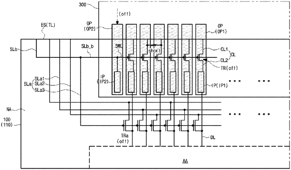
1. A display device, comprising:
a substrate including a display area and a non-display area, the display area including pixels;
data lines extending into the display area and connected to the pixels;
first input pads in the non-display area and respectively directly connected to the data lines on a one-to-one basis;
a plurality of switching transistors in the non-display area respectively directly connected to the first input pads on a one-to-one basis to be between the first input pads and a first side of the substrate such that each first input pad is connected between a respective switching transistor among the plurality of switching transistor and a respective data line;
a plurality of first connection lines respectively connected to ones of the plurality of switching transistors on a one-to-one basis, each first connection line extending to an edge of the substrate at the first side on a one-to-one basis; and
a second input pad in the non-display area and connected to a gate electrode of each switching transistor of the plurality of switching transistors through a switching line; and
a circuit film connected to the first side of the substrate and including first and second output pads, wherein the first output pad is connected to and transmits a data signal for displaying an image to the first input pads, and the second output pad is connected to and transmits a switching signal to the second input pad.
|