| CPC H10K 59/126 (2023.02) [G09G 3/3225 (2013.01); H10K 59/131 (2023.02); H10K 71/00 (2023.02)] | 13 Claims |
|
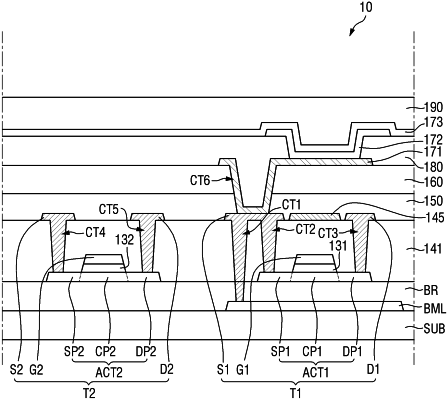
1. A display device comprising:
a substrate;
a driving transistor including a first active layer and a switching transistor including a second active layer, the first active layer and the second active layer being disposed on the substrate;
a first gate insulating layer disposed on the first active layer of the driving transistor and a second gate insulating layer disposed on the second active layer of the switching transistor;
a first gate electrode and a second gate electrode disposed on the first gate insulating layer and the second gate insulating layer to overlap the first active layer of the driving transistor and the second active layer of the switching transistor, respectively;
a first interlayer insulating layer disposed on the first gate electrode and the second gate electrode; and
a second interlayer insulating layer disposed on the first interlayer insulating layer to overlap the first active layer without overlapping the second active layer in a plan view,
wherein the second insulating layer is disposed between a first source electrode and a first drain electrode which are respectively connected to a source region and a drain region of the first active layer, and
wherein the second interlayer insulating layer is spaced apart from at least one of the first source electrode and the first drain electrode.
|