| CPC H10K 50/8445 (2023.02) [H10K 50/844 (2023.02); H10K 50/858 (2023.02); H10K 59/12 (2023.02); H10K 59/123 (2023.02); H10K 59/124 (2023.02); H10K 71/00 (2023.02); H10K 59/1201 (2023.02); H10K 2102/311 (2023.02)] | 11 Claims |
|
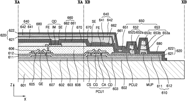
1. A display apparatus comprising:
a substrate having a display area and a peripheral area around the display area;
a display device on the display area;
an encapsulating layer covering the display device, and comprising a first inorganic layer and a second inorganic layer on the first inorganic layer, the first inorganic layer on the display area and extending to a portion of the peripheral area;
a blocking member disposed on the peripheral area and comprising a first blocking member and a second blocking member; and
a conductive member disposed below the second blocking member, a bottom surface of the conductive member and a bottom surface of the second blocking member being on an upper surface of a same layer,
wherein the first inorganic layer directly contacts the second inorganic layer in at least a region of the peripheral area.
|