| CPC H10K 50/844 (2023.02) [H10K 50/868 (2023.02); H10K 71/00 (2023.02)] | 23 Claims |
|
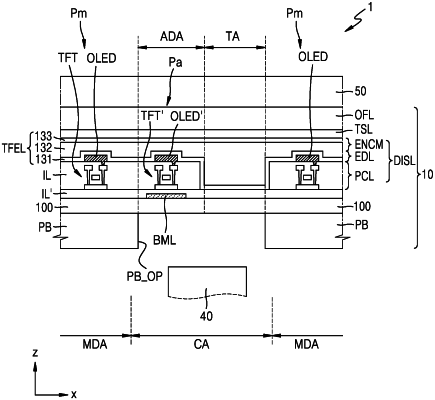
1. A display apparatus comprising:
a substrate including a main display area and a component area, the component area including an auxiliary display area and a transmission area;
main display elements disposed in the main display area;
auxiliary display elements disposed in the component area, wherein the transmission area does not include the auxiliary display elements;
a thin-film encapsulation layer covering the main display elements and the auxiliary display elements; and
an optical functional layer disposed on the thin-film encapsulation layer and including a polarization layer,
wherein the polarization layer includes a first portion disposed in the transmission area and a second portion disposed in the main display area and the auxiliary display area,
wherein the polarization layer does not include any openings in the first portion, and
wherein entireties of the first portion and the second portion are disposed on a same layer as each other.
|