| CPC H10B 63/845 (2023.02) [H10B 61/00 (2023.02); H10N 50/01 (2023.02); H10N 50/80 (2023.02); H10N 70/066 (2023.02); H10N 70/841 (2023.02)] | 9 Claims |
|
1. A method of manufacturing an electronic device including a semiconductor memory, the method comprising:
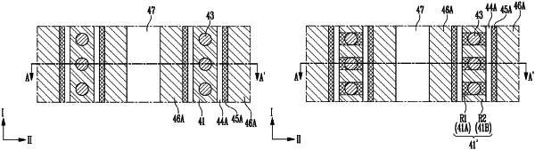
forming a stacked structure including sacrificial layers and insulating layers stacked alternately with each other;
forming conductive pillars passing through the stacked structure;
forming a slit passing through the stacked structure;
forming openings by partially removing the sacrificial layers through the slit;
forming variable resistance layers in the openings;
forming conductive layers in the openings; and
forming material layers including conductive areas and insulating areas by applying an electric field to portions of the sacrificial layers.
|