| CPC H10B 51/20 (2023.02) [H10B 51/10 (2023.02)] | 15 Claims |
|
1. A method of manufacturing a semiconductor device, the method comprising:
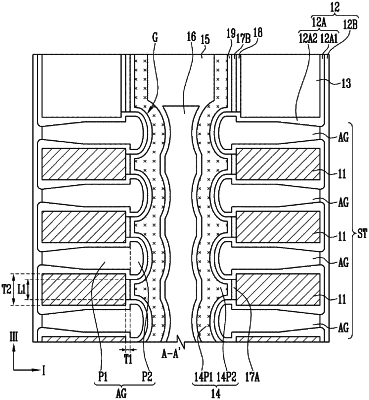
forming a stacked structure including first material layers and second material layers stacked alternately with each other;
forming a first opening passing through the stacked structure and including an inner wall where the second material layers protrude into the first opening more than the first material layers;
sequentially forming a sacrificial layer, a first dielectric layer, a ferroelectric layer and a channel layer over the inner wall of the first opening;
forming second openings by selectively etching the second material layers;
etching the sacrificial layer through the second openings to expose the first dielectric layer;
forming first dielectric patterns by etching the first dielectric layer through the second openings; and
forming gaps in the second openings by sealing the second openings.
|