| CPC H10B 43/50 (2023.02) [H01L 21/76805 (2013.01); H01L 21/76895 (2013.01); H01L 23/535 (2013.01); H10B 41/27 (2023.02); H10B 41/41 (2023.02); H10B 41/50 (2023.02); H10B 43/27 (2023.02); H10B 43/40 (2023.02)] | 10 Claims |
|
1. A semiconductor device, comprising:
a peripheral circuit region on a first substrate and including circuit elements;
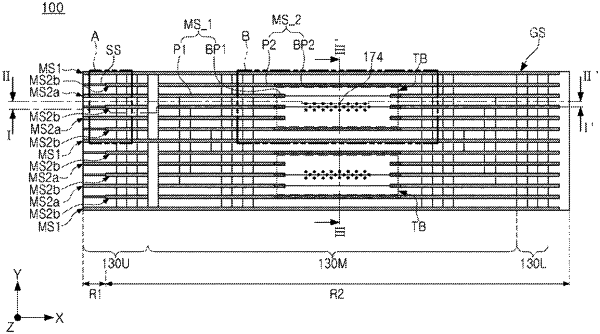
a stack structure provided on a second substrate disposed on the peripheral circuit region and including:
gate electrodes stacked to be spaced apart from each other in a first direction perpendicular to an upper surface of the second substrate on a first region of the second substrate and extending while having a staircase shape in a cross-sectional view in a second direction perpendicular to the first direction on a second region of the second substrate, and
interlayer insulating layers stacked alternately with the gate electrodes;
a channel structure penetrating through the stack structure, extending vertically on the second substrate, and including a channel layer;
a separation structure penetrating through the stack structure and extending in the second direction, and including a first separation pattern and a pair of second separation patterns disposed to be parallel to the first separation pattern;
a through-region disposed between the pair of second separation patterns and including a lower through-insulating layer penetrating through the second substrate, and the interlayer insulating layers and sacrificial insulating layers sequentially stacked on the lower through-insulating layer; and
through-contact plugs extending in the first direction through the through-region and electrically connected to the circuit elements of the peripheral circuit region,
wherein the sacrificial insulating layers have side surfaces opposing the gate electrodes, and
wherein an end portion of the first separation pattern protrudes further than at least some of the side surfaces of the sacrificial insulating layers toward the through-region.
|