| CPC H10B 43/40 (2023.02) [H01L 23/5226 (2013.01); H01L 23/535 (2013.01); H01L 23/562 (2013.01); H10B 43/27 (2023.02)] | 14 Claims |
|
1. A semiconductor device comprising:
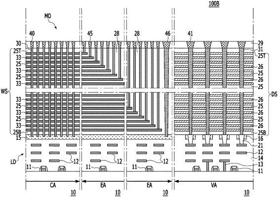
a substrate having a cell area and a via area;
a transistor and a logic interconnection disposed over the substrate;
a lower insulating layer covering the transistor and the logic interconnection;
a common source region on the lower insulating layer in the cell area;
a support pattern disposed on the lower insulating layer in the via area;
a lower via plug having a side surface in contact with the support pattern and a bottom surface in contact with the logic interconnection in the via area;
a word line stack disposed on the common source region in the cell area;
a dielectric layer stack disposed on the support pattern and the lower insulating layer in the via area;
a plurality of vertical channel pillar penetrating the word line stack to be commonly connected to the common source region in the cell area;
an upper via plug penetrating the dielectric layer stack to be aligned in a vertical direction with the lower via plug in the via area,
wherein the support pattern is a conductor; and
wherein the semiconductor device further comprises:
a plurality of support patterns arranged to be spaced apart from each other in a horizontal direction by a portion of the lower insulating layer,
a plurality of lower via plugs, each of the plurality of lower via plugs in directly contact with each of the plurality of support patterns, respectively; and
wherein the support pattern has a pair of segments shaped to contact at least two side surfaces of the lower via plug having a plurality of side surfaces.
|