| CPC H10B 43/27 (2023.02) [H01L 23/5226 (2013.01); H01L 23/528 (2013.01); H01L 29/40114 (2019.08); H01L 29/40117 (2019.08); H01L 29/66545 (2013.01); H10B 41/10 (2023.02); H10B 41/27 (2023.02); H10B 41/40 (2023.02); H10B 43/10 (2023.02); H10B 43/40 (2023.02)] | 18 Claims |
|
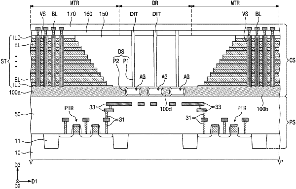
1. A three-dimensional semiconductor memory device, comprising:
horizontal patterns disposed on a peripheral circuit structure and spaced apart from each other in a first direction parallel to a top surface of a substrate;
memory structures provided on the horizontal patterns, respectively, each of the memory structures comprising memory cells, which are three-dimensionally arranged;
penetrating insulating patterns, each being provided between adjacent ones of the horizontal patterns and being spaced apart from each other in a second direction crossing the first direction, each penetrating insulating pattern abutting side surfaces of the adjacent horizontal patterns;
through plugs extending through a corresponding penetrating insulating pattern to electrically connect the memory structures to the peripheral circuit structure; and
first and second separation structures disposed between the horizontal patterns, spaced apart from each other in the first direction and extending between the penetrating insulating patterns in the second direction and connected to adjacent ones of the penetrating insulating patterns,
wherein the horizontal patterns are portions of a first material layer,
wherein each of the penetrating insulating patterns penetrates the first material layer and have opposite borders that extend between side surfaces of the horizontal patterns and that are defined, at least in part, by the first material layer, and
wherein the three-dimensional semiconductor memory device comprises a dummy horizontal pattern, which is disposed between the penetrating insulating patterns and between the first and second separation structures.
|