| CPC H10B 12/485 (2023.02) [H10B 12/482 (2023.02)] | 11 Claims |
|
1. A method of manufacturing a semiconductor structure, comprising:
providing a substrate;
forming a bitline contact hole located in the substrate, and forming a non-metal conductive layer to cover a surface of the substrate and fill the bitline contact hole, the non-metal conductive layer having a first opening formed therein, the first opening aligned with the bitline contact hole;
forming a metal conductive layer to cover a surface of the non-metal conductive layer;
forming an insulation layer to cover a surface of the metal conductive layer; and
etching the insulation layer, the metal conductive layer, and the non-metal conductive layer to form a bitline structure;
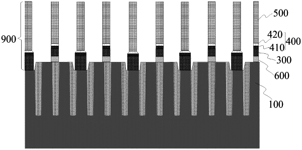
wherein the metal conductive layer and the non-metal conductive layer collectively form a bitline, and the bitline located in the bitline contact hole has a width not less than that of the bitline located outside of the bitline contact hole;
wherein forming the bitline contact hole and the non-metal conductive layer comprises:
forming a first sublayer of non-metal conductive material on the substrate;
etching the first sublayer of non-metal conductive material and the substrate to form the bitline contact hole, a retained first sublayer of non-metal conductive material serving as a first sublayer of the non-metal conductive layer; and
forming a second sublayer of the non-metal conductive layer to cover the bitline contact hole, and a top of the second sublayer of the non-metal conductive layer is lower than a top of the first sublayer of the non-metal conductive layer, the first and second sublayers of the non-metal conductive layer collectively forming the non-metal conductive layer.
|