| CPC H05K 1/0271 (2013.01) [H01L 21/50 (2013.01); H01L 23/5385 (2013.01); H01L 23/5386 (2013.01); H01L 24/14 (2013.01); H01L 2021/60097 (2013.01); H01L 2224/16225 (2013.01)] | 12 Claims |
|
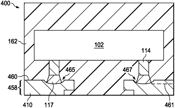
1. An apparatus, comprising:
a package substrate having a planar die mount surface;
recesses extending into the planar die mount surface; and
a semiconductor device die flip chip mounted to the package substrate on the planar die mount surface, the semiconductor device die having post connects having proximate ends on bond pads on an active surface of the semiconductor device die, and extending to distal ends away from the semiconductor device die having solder bumps, wherein the solder bumps form solder joints to the package substrate within the recesses, wherein the package substrate is a metal lead frame made entirely of metal.
|