| CPC H05K 1/0218 (2013.01) [G06F 3/0412 (2013.01); H05K 1/028 (2013.01); H05K 1/144 (2013.01); H05K 1/147 (2013.01); G06F 3/0443 (2019.05); H05K 2201/041 (2013.01); H05K 2201/10128 (2013.01)] | 18 Claims |
|
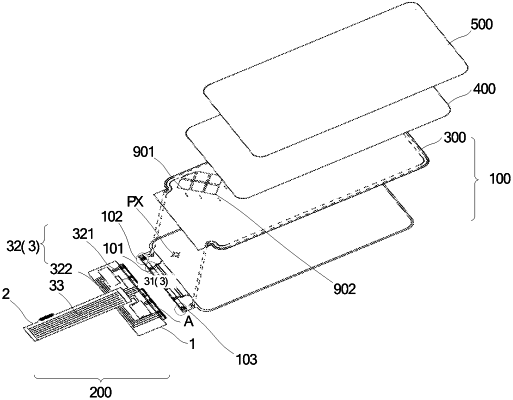
1. A flexible printed circuit board, comprising a main flexible printed circuit board and an adaptor flexible printed circuit board; wherein
the main flexible printed circuit board is a single-layer board or a double-layer board, and comprises:
a bonding region configured for bonding with a display panel;
a component arranging region configured for arranging a control component;
a first connection region configured for connecting with the adaptor flexible printed circuit board;
a first signal line disposed between the component arranging region and the first connection region; and
a second signal line disposed between the component arranging region and the bonding region;
the adaptor flexible printed circuit board has an outline different from an outline of the main flexible printed circuit board, the adaptor flexible printed circuit board is a single-layer board or a double-layer board, and the adaptor flexible printed circuit board comprises:
a second connection region configured for connecting with the main flexible printed circuit board;
a third connection region configured for connecting with a printed circuit board; and
a third signal line disposed between the second connection region and the third connection region;
wherein an orthographic projection of the second connection region on the main flexible printed circuit board completely falls within a region range of the main flexible printed circuit board, and an orthographic projection of the third connection region on a plane of the main flexible printed circuit board does not fall within the region range of the main flexible printed circuit board;
the main flexible printed circuit board and the adaptor flexible printed circuit board are connected through the first connection region and the second connection region, an orthographic projection of the third signal line on the main flexible printed circuit board and the second signal line have an overlapping region; wherein
in the overlapping region, an electromagnetic shielding structure is at least disposed on a side of the main flexible printed circuit board facing the adaptor flexible printed circuit board or on a side of the adaptor flexible printed circuit board facing the main flexible printed circuit board;
wherein the adaptor flexible printed circuit board comprises a third substrate layer, a fourth conductive layer disposed on a fourth surface of the third substrate layer, and a fifth conductive layer disposed on a fifth surface of the third substrate layer opposite to the fourth surface, wherein the fifth surface is a surface of the third substrate layer close to the main flexible printed circuit board, and the fourth conductive layer comprises the third signal line; and
the electromagnetic shielding structure is disposed on the side of the adaptor flexible printed circuit board facing the main flexible printed circuit board, and in the overlapping region, the electromagnetic shielding structure comprises a second conductive part disposed in the fifth conductive layer, wherein the second conductive part is grounded.
|