| CPC H05B 3/141 (2013.01) [F23Q 7/001 (2013.01); H05B 3/18 (2013.01); H05B 3/28 (2013.01); H05B 3/48 (2013.01); H05B 2203/027 (2013.01)] | 6 Claims |
|
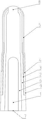
1. A ceramic electric heating element wherein:
the ceramic electric heating element has six layers that include, from the inside out, an inner conducting layer (1), an inner resistive layer (6), an inner insulating layer (2), an outer resistive layer (3), an outer conducting layer (4), and an outer insulating layer (5), respectively;
an upper tip portion of the ceramic electric heating element is completely wrapped by the outer insulating layer;
the inner conducting layer (1) is located in the center of the ceramic electric heating element;
the inner resistive layer (6) wraps the inner conducting layer (1) on the outside;
the inner insulating layer (2) wraps the inner resistive layer (6) on the outside, and the inner insulating layer (2) is divided into two segments, with the peripheral profile of the lower segment being greater than that of the upper segment;
the outer resistive layer (3) wraps the upper part of the inner insulating layer (2) on the outside, and the outer resistive layer (3) is divided into two segments, with the peripheral profile of the upper segment of the outer resistive layer (3) being less than that of the lower segment of the inner insulating layer (2);
the outer conducting layer (4) wraps the lower segment of the outer resistive layer (3) on the outside, and the outer conducting layer (4) is divided into two segments, with the peripheral profile of the lower segment equaling to that of the lower segment of the inner insulating layer (2), and the peripheral profile of the upper segment equaling to that of the upper segment of the outer resistive layer (6);
the outer insulating layer (5) wraps the upper segment of the outer conducting layer (4) and the upper segment of the outer resistive layer (3) on the outside, with the peripheral profile of a lower segment of the outer insulating layer (5) equaling to that of the lower segment of the outer conducting layer (4);
the lower part of the inner conducting layer (1) has a spot (7) where a central electrode is located, the upper end of the inner resistive layer (6) has a connecting hole (8), and the outside of the lower part of the outer conducting layer (4) has a spot (9) where a side electrode is connected;
the spot (7) where the central electrode is located is solid; and
an electrically conductive ceramic electrode is welded to the spot (7).
|