| CPC H04B 1/123 (2013.01) [H04B 1/0475 (2013.01); H04B 1/1027 (2013.01)] | 9 Claims |
|
1. An adaptive method for a multi-order multi-band anti-interference intelligent Ultra Wide Band (UWB) antenna, characterized by comprising:
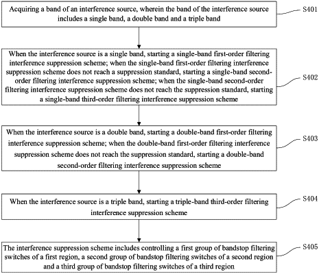
acquiring a band of an interference source, wherein the band of the interference source comprises a single band, a double band and a triple band;
when the interference source is a single band, starting a single-band first-order filtering interference suppression scheme; when the single-band first-order filtering interference suppression scheme does not reach a suppression standard, starting a single-band second-order filtering interference suppression scheme; when the single-band second-order filtering interference suppression scheme does not reach the suppression standard, starting a single-band third-order filtering interference suppression scheme;
when the interference source is a double band, starting a double-band first-order filtering interference suppression scheme; when the double-band first-order filtering interference suppression scheme does not reach the suppression standard, starting a double-band second-order filtering interference suppression scheme;
when the interference source is a triple band, starting a triple-band third-order filtering interference suppression scheme;
wherein the interference suppression schemes comprise controlling switching of a first group of bandstop filtering switches of a first region, a second group of bandstop filtering switches of a second region and a third group of bandstop filtering switches of a third region;
the first group of bandstop filtering switches comprises a first filter, a second filter and a third filter; states formed by the first, second and third filters after switching comprise forming a bandstop filtering state with a center frequency of 3.5 GHz, forming a bandstop filtering state with a center frequency of 4.9 GHz, forming a bandstop filtering state with a center frequency of 5.5 GHz, and forming a state where no filtering is formed;
the second group of bandstop filtering switches comprises a fourth filter, a fifth filter and a sixth filter; states formed by the fourth, fifth and sixth filters after switching comprise forming a bandstop filtering state with a center frequency of 3.5 GHz, forming a bandstop filtering state with a center frequency of 4.9 GHz, forming a bandstop filtering state with a center frequency of 5.5 GHz, and forming a state where no filtering is formed;
the third group of bandstop filtering switches comprises a seventh filter, an eighth filter and a ninth filter; and states formed by the seventh, eighth and ninth filters after switching comprise forming a bandstop filtering state with a center frequency of 3.5 GHz, forming a bandstop filtering state with a center frequency of 4.9 GHz, forming a bandstop filtering state with a center frequency of 5.5 GHz, and forming a state where no filtering is formed.
|