| CPC H04B 1/0064 (2013.01) [H01Q 1/243 (2013.01); H01Q 5/50 (2015.01); H01Q 21/08 (2013.01); H05K 1/0243 (2013.01); H05K 1/0277 (2013.01); H05K 7/1427 (2013.01); H05K 2201/10098 (2013.01)] | 15 Claims |
|
1. An electronic device comprising:
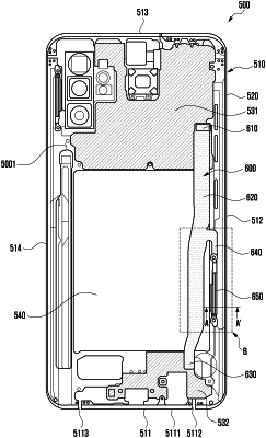
a housing comprising a first lateral surface, a second lateral surface, a third lateral surface, and a fourth lateral surface having an inner space therein;
a printed circuit board (PCB) disposed in the inner space of the housing;
a first antenna structure comprising at least one conductive portion disposed at a position spaced apart from the PCB in a part of the first lateral surface of the housing, and configured for transmitting and/or receiving a radio signal in a first frequency band;
at least one second antenna structure disposed at a position spaced apart from the PCB within the inner space and affixed to the second lateral surface of the housing perpendicular to the first lateral surface, and configured for transmitting and/or receiving a radio signal in a second frequency band different from the first frequency band; and
a flexible substrate electrically connecting the PCB and the first antenna structure, and including:
a first connecting portion electrically connected to the PCB;
an interconnecting portion extended from the first connecting portion to the first antenna structure;
at least one branch portion branched from at least a part of the interconnecting portion, and extended to the at least one second antenna structure;
at least one first conductive path disposed in the interconnecting portion, and electrically connecting the first connecting portion and the first antenna structure; and
at least one second conductive path disposed in the interconnecting portion and the at least one branch portion, and electrically connecting the first connecting portion and the at least one second antenna structure.
|