| CPC H04B 1/0007 (2013.01) [H04B 1/0053 (2013.01); H04B 1/403 (2013.01); H04B 1/588 (2013.01)] | 27 Claims |
|
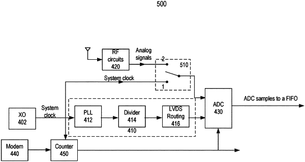
1. A method for determining an analog-to-digital converter (ADC) output timing in a user equipment, comprising:
operating a switch in a first mode to route a system clock from an oscillator to an input of the ADC;
determining a first ADC output timing based on a first set of ADC samples generated by the ADC;
operating the switch in a second mode to route analog signals from a transceiver of the user equipment to the input of the ADC; and
obtaining a second set of ADC samples generated by the ADC based on the analog signals.
|