| CPC H03K 17/6871 (2013.01) [G06N 10/40 (2022.01)] | 20 Claims |
|
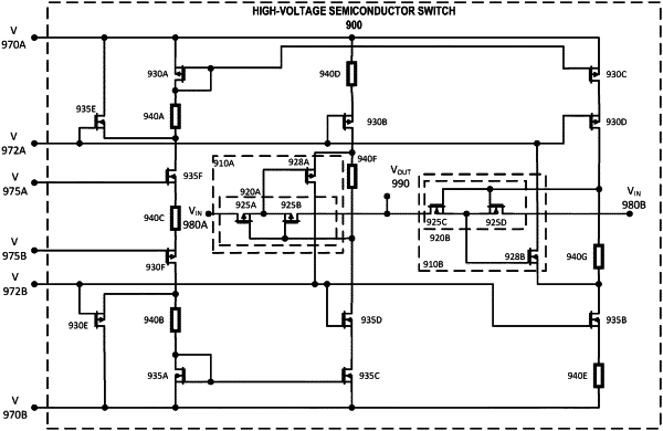
1. A high-voltage semiconductor switch comprising:
a first switch subcircuit comprising one or more FET circuits and a first voltage-shifting FET, wherein a first FET circuit of the first switch subcircuit comprises a first FET and a second FET;
a second switch sub circuit comprising one or more FET circuits and a second voltage-shifting transistor, wherein a first FET circuit of the second switch subcircuit comprises a third FET and a fourth FET;
wherein each of the first FET, the second FET, the third FET, the fourth FET, the first voltage-shifting FET, and the second voltage-shifting transistor comprises a gate, a drain, and a source;
wherein:
the gate of the first FET and the gate of the second FET are connected to a gate terminal of the first switch subcircuit;
the gate of the third FET and the gate of the fourth FET are connected to a gate terminal of the second switch subcircuit;
the source of the first FET, the source of the second FET, and the gate of the first voltage-shifting FET are connected; and
the source of the third FET, the source of the fourth FET, and the gate of the second voltage-shifting FET are connected; and
the high-voltage semiconductor switch further comprising:
an input terminal connected to the drain of the first FET and the drain of the fourth FET; and
an output terminal connected to the drain of the second FET and the drain of the third FET.
|