| CPC H03K 17/567 (2013.01) [H01L 27/0783 (2013.01); H03K 19/084 (2013.01)] | 10 Claims |
|
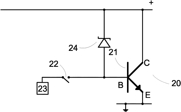
1. A circuit comprising:
a bipolar transistor;
a base terminal of the bipolar transistor being switchably connectable to a signal source;
a diode having a first terminal connected to the base terminal of the bipolar transistor, and a second terminal connected to a reference voltage;
the circuit arranged such that when the signal source is not connected to the base terminal of the bipolar transistor, a voltage applied at an emitter terminal of the bipolar transistor causes a current flow through the base terminal of the bipolar transistor and through the diode such that the bipolar transistor is in an ON state;
an impedance of the signal source being lower than an impedance of the bipolar transistor through emitter and base terminals of the bipolar junction transistor; and
the diode being selected to provide a current limiting function such that when the signal source is connected to the base terminal of the bipolar transistor, current flow through the base terminal reduces such that the bipolar transistor switches to an OFF state.
|