| CPC H03F 1/26 (2013.01) [G11C 7/062 (2013.01); G11C 7/08 (2013.01); G11C 7/1069 (2013.01); G11C 7/12 (2013.01); H03F 2200/375 (2013.01)] | 18 Claims |
|
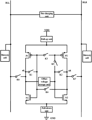
1. A Sense Amplifier (SA), comprising:
an amplifier circuit;
an offset voltage storage circuit electrically connected to the amplifier circuit, and configured to store an offset voltage of the amplifier circuit in an offset elimination stage of the SA; and
a load compensation circuit electrically connected to the amplifier circuit, and configured to compensate a difference between loads of the amplifier circuit in an amplification stage of the SA,
wherein the amplifier circuit comprises:
a first P-channel Metal Oxide Semiconductor (PMOS) transistor;
a second PMOS transistor, a source of the second PMOS transistor being connected to a source of the first PMOS transistor;
a first N-channel Metal Oxide Semiconductor (NMOS) transistor, a drain of the first NMOS transistor being connected to a drain of the first PMOS transistor and a first end of the offset voltage storage circuit, and a gate of the first NMOS transistor being connected to a gate of the first PMOS transistor; and
a second NMOS transistor, a drain of the second NMOS transistor being connected to a drain of the second PMOS transistor, a source of the second NMOS transistor being connected to a source of the first NMOS transistor, and a gate of the second NMOS transistor being connected to a second end of the offset voltage storage circuit,
wherein in the offset elimination stage of the SA, the first PMOS transistor and the second PMOS transistor are configured as a current mirror, and each of the first NMOS transistor and the second NMOS transistor is configured as a diode connection mode, to store the offset voltage of the amplifier circuit in the offset voltage storage circuit.
|