| CPC H02M 5/2932 (2021.05) [B60L 50/16 (2019.02); H02M 5/14 (2013.01); B60L 2200/26 (2013.01); B60L 2210/20 (2013.01)] | 7 Claims |
|
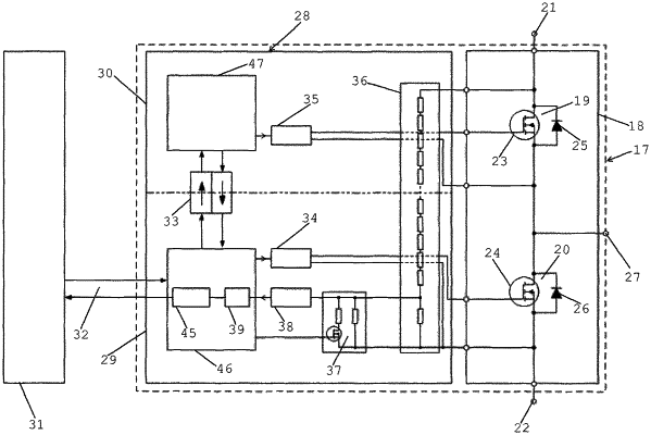
1. A voltage source converter comprising
a half bridge (18) with two current valves (19, 20) connected in series and configured to be connected to opposite poles (21, 22) of a DC source/load, each said current valve comprising a semiconductor device (23, 24) of turn-off type and a rectifying diode (25, 26) connected in anti-parallel therewith, a midpoint of the half bridge between the two current valves forming an AC side (27) of the converter and being configured to be connected to an AC load/source,
two gate drive members (29, 30) each comprising a logic device (46, 47) and a gate drive stage (34, 35) configured to control the semiconductor device (23, 24) of a current valve (19, 20) each to turn on and off according to control signals from a converter control device (31),
said converter control device (31) configured to send control signals to said gate drive members (29, 30) for controlling the operation of the converter according to a Pulse Width Modulation pattern for creating an AC fundamental voltage and current on said AC side, and
an arrangement configured to carry out voltage measurements for providing a value of the DC voltage between said opposite poles (21, 22) to a first said logic device configured to send information about said DC voltage value to the converter control device (31),
wherein said two gate drive members (29, 30) form gate drive parts of one gate drive unit (28) in common to both current valves (19, 20),
said gate drive unit contains an electrically isolating two-way communication link (33) interconnecting said gate drive members,
said arrangement is included in said gate drive unit (28) and comprises a voltage divider (36) connected across the two current valves (19, 20) to measure the entire DC voltage between said opposite poles (21, 22), and
the converter control device (31) is configured to calculate and send said control signals to the gate drive unit (28) based on the result of a said measurement carried out by said arrangement,
said first gate drive member (29) is configured to send information about the DC voltage measured also directly to the second gate drive member (30),
both gate drive members (29, 30) are configured to use information about this voltage to optimize the switching of the semiconductor device (23, 24) of the respective current valve (19, 20),
said voltage divider (36) has an output with one of said poles (21, 22) as reference potential,
said output is connected to processing parts (37, 38, 39, 45) which are included in said first gate drive member (29), and
said first gate drive member (29) is configured to directly use the value of the DC voltage measured by the arrangement for the control of said semiconductor device (24).
|