| CPC H01P 1/2002 (2013.01) | 19 Claims |
|
1. A RF dielectric filter comprising:
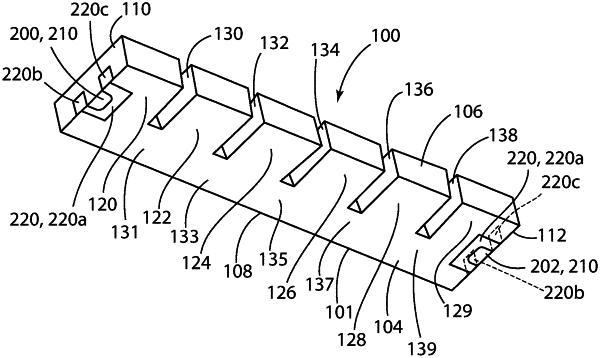
a block of dielectric material including a plurality of exterior surfaces including top and bottom exterior longitudinal surfaces, opposed side exterior longitudinal surfaces, and opposed exterior end surfaces;
at least a first RF signal input/output pad extending between the bottom exterior surface and one of the opposed side exterior longitudinal surfaces or one of the opposed exterior end surfaces;
wherein the at least first RF signal input/output pad comprises:
an elongate strip of conductive material extending between the bottom exterior surface and one of the opposed side exterior longitudinal surfaces or one of the opposed exterior end surfaces; and
a generally U-shaped strip of dielectric material surrounding all the sides of the elongate strip of conductive material except for a top side of the elongate strip of conductive material located on the one of the opposed side exterior longitudinal surfaces or the one of the opposed exterior end surfaces; and
wherein a width of each of opposed portions of the strip of dielectric material located on the one of the opposed side exterior longitudinal surfaces or the one of the opposed exterior end surfaces is greater than a width of each of lengths of the strip of dielectric material located on the bottom exterior surface that extend to the opposing portions.
|