| CPC H01L 31/1868 (2013.01) [H01L 31/02366 (2013.01); H01L 31/03685 (2013.01); H01L 31/068 (2013.01); H01L 31/1824 (2013.01)] | 20 Claims |
|
1. A solar cell, comprising:
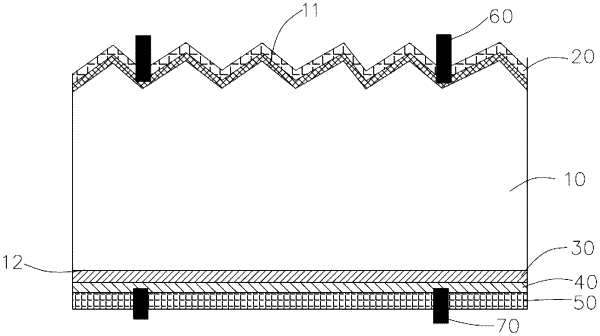
an N-type semiconductor substrate, wherein a rear surface of the N-type semiconductor substrate includes a non-pyramid-shaped microstructure, and the non-pyramid-shaped microstructure includes two or more first substructures at least partially stacked on one another and two or more second substructures adjacent to one another and not stacked on one another, a top surface of the first substructure and a top surface of second first substructure are both a polygonal plane; and wherein a front surface of the N-type semiconductor substrate includes a pyramid-shaped microstructure, the pyramid-shaped microstructure includes a top portion away from the front surface of the semiconductor substrate and a bottom portion close to the front surface of the semiconductor substrate, and in a direction away from the front surface and perpendicular to the front surface, a distance between the top portion and the bottom portion of the pyramid-shaped microstructure is less than or equal to 5 μm;
a first passivation layer located on the pyramid-shaped microstructure of the front surface of the N-type semiconductor substrate;
a tunnel oxide layer located on the non-pyramid-shaped microstructure of the rear surface of the N-type semiconductor substrate;
a doped conductive layer located on a surface of the tunnel oxide layer; and
a second passivation layer located on a surface of the doped conductive layer.
|