| CPC H01L 31/1844 (2013.01) [H01L 31/0304 (2013.01); H01L 31/03046 (2013.01); H01L 31/0352 (2013.01); H01L 31/035236 (2013.01); H01L 31/102 (2013.01); H01L 31/18 (2013.01); H01L 33/00 (2013.01); Y02P 70/50 (2015.11)] | 15 Claims |
|
1. A preparation method of a detector material, comprising the following steps:
(1) growing a gallium compound on a surface of an initial substrate to obtain a buffer layer, wherein the initial substrate is a gallium arsenide substrate; and the gallium compound is gallium arsenide or gallium antimonide;
(2) depositing silicon dioxide on a surface of the buffer layer to obtain a silicon dioxide film;
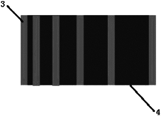
(3) conducting photolithography and etching on the silicon dioxide film sequentially to obtain a strip growth layer, wherein widths of strip growth regions of the strip growth layer change continuously; and
(4) growing a quantum well or superlattice on the strip growth layer to obtain the detector material, wherein the quantum well is an InxGaAs/GaAs quantum well, and the superlattice is an InAs/GaSb superlattice.
|