| CPC H01L 29/78606 (2013.01) [H01L 21/02178 (2013.01); H01L 21/02565 (2013.01); H01L 29/66969 (2013.01); H01L 29/7869 (2013.01)] | 20 Claims |
|
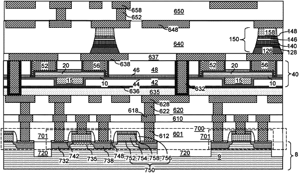
1. A semiconductor device comprising:
an insulating matrix layer including an opening therein and overlying a substrate;
a hydrogen-blocking dielectric barrier layer extending over a horizontal plane including a bottom surface of the insulating matrix layer;
a gate electrode located within the opening on the hydrogen-blocking dielectric barrier layer, wherein the hydrogen-blocking dielectric barrier layer comprises a first horizontally-extending portion that underlies the gate electrode;
a stack of a gate dielectric and a semiconducting metal oxide plate overlying a top surface of the gate electrode and horizontally-extending portions of the hydrogen-blocking dielectric barrier layer that overlie the insulating matrix layer; and
a source electrode and a drain electrode contacting respective portions of a top surface of the semiconducting metal oxide plate.
|