| CPC H01L 29/7835 (2013.01) [H01L 29/0653 (2013.01); H01L 29/0847 (2013.01); H01L 29/1083 (2013.01)] | 5 Claims |
|
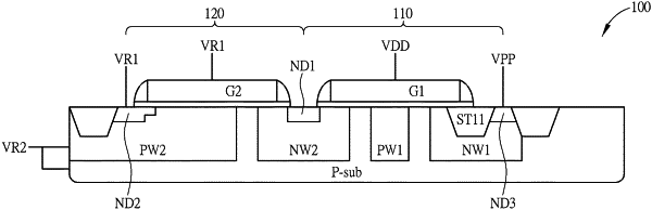
4. A switch device, comprising:
a substrate;
a first gate structure;
a first well of a first conduction type formed in the substrate and partly under a first side of the first gate structure;
a second gate structure;
a second well of a second conduction type formed in the substrate and under the first gate structure and the second gate structure;
a first doped region of the first conduction type formed in the second well and between a second side of the first gate structure and a first side of the second gate structure; and
a second doped region of the first conduction type formed in the second well and adjacent to a second side of the second gate structure;
wherein the first conduction type and the second conduction type are of different doping polarity;
wherein when the switch device is in a second state:
the second well receives a fourth reference voltage;
the second doped region receives a first input voltage;
the second gate structure receives a second input voltage; and
the first gate structure receives an operation voltage; and
wherein an absolute value of a fifth voltage drop between the second input voltage and the fourth reference voltage and an absolute value of a sixth voltage drop between the operation voltage and the fourth reference voltage are greater than an absolute value of a seventh voltage drop between the first input voltage and the fourth reference voltage, and the absolute value of the seventh voltage drop is greater than or equal to zero.
|