| CPC H01L 29/7825 (2013.01) [H01L 29/0607 (2013.01); H01L 29/0865 (2013.01); H01L 29/0882 (2013.01); H01L 29/4236 (2013.01); H01L 29/7835 (2013.01)] | 9 Claims |
|
1. A semiconductor device comprising:
a semiconductor substrate;
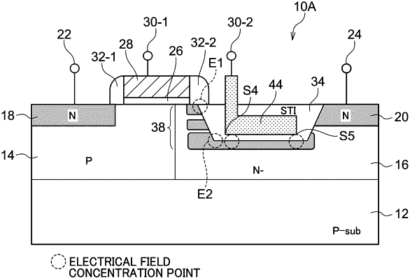
a source region having a first conductivity type formed within one main face of the semiconductor substrate;
a drain region having the first conductivity type formed within the one main face;
a gate electrode formed above the one main face with an insulating film therebetween;
a shallow trench isolation (STI) layer within the one main face and including one end adjacent the gate electrode;
first and second sidewalls on opposite sides of the gate electrode; and
an L-shaped electrical field weakening portion located within the STI layer, the L-shaped electrical field weakening portion weakens an electrical field generated between the source region and the drain region,
wherein the L-shaped electrical field weakening portion includes a corner section, a horizontal section and a vertical section,
wherein the horizontal section extends horizontally from the corner section, and the vertical section extends vertically upward from the corner section,
wherein the corner section and the horizontal section of the L-shaped electrical field weakening portion are buried within the STI layer below an upper surface of the STI layer, and the vertical section of the L-shaped electrical field weakening portion protrudes upwardly through the upper surface of the STI layer,
wherein the first sidewall extends partially over the source region, and
wherein the second sidewall extends partially over the one end of the STI layer.
|