| CPC H01L 29/66795 (2013.01) [H01L 21/02532 (2013.01); H01L 21/02603 (2013.01); H01L 21/823431 (2013.01); H01L 21/823807 (2013.01); H01L 21/823814 (2013.01); H01L 21/823864 (2013.01); H01L 21/823878 (2013.01); H01L 29/0673 (2013.01); H01L 29/0847 (2013.01); H01L 29/1033 (2013.01); H01L 29/42356 (2013.01); H01L 29/66439 (2013.01); H01L 29/66545 (2013.01); H01L 29/66553 (2013.01); H01L 29/6681 (2013.01); H01L 29/775 (2013.01); H01L 29/785 (2013.01); H01L 2029/7858 (2013.01)] | 20 Claims |
|
1. A semiconductor structure, comprising:
a substrate;
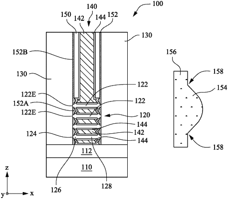
multiple separate semiconductor nanowire strips vertically stacked over the substrate;
a semiconductor region adjacent to and laterally contacting each of the multiple separate semiconductor nanowire strips;
a gate structure at least partially over the multiple separate semiconductor nanowire strips; and
a first dielectric structure laterally between the semiconductor region and the gate structure, the first dielectric structure having a hat-shaped profile, wherein the hat-shaped profile including a dome-shaped portion and a brim-shaped portion.
|