US 11,929,424 B2
Semiconductor device and method for forming the same
Yi-Chen Lo, Hsinchu County (TW); Li-Te Lin, Hsinchu (TW); and Pinyen Lin, Rochester, NY (US)
Assigned to TAIWAN SEMICONDUCTOR MANUFACTURING CO., LTD., Hsinchu (TW)
Filed by TAIWAN SEMICONDUCTOR MANUFACTURING CO., LTD., Hsinchu (TW)
Filed on Jul. 26, 2022, as Appl. No. 17/873,962.
Application 16/937,901 is a division of application No. 16/136,339, filed on Sep. 20, 2018, granted, now 10,741,671, issued on Aug. 11, 2020.
Application 17/873,962 is a continuation of application No. 16/937,901, filed on Jul. 24, 2020, granted, now 11,424,341.
Claims priority of provisional application 62/591,237, filed on Nov. 28, 2017.
Prior Publication US 2022/0359724 A1, Nov. 10, 2022
Int. Cl. H01L 21/033 (2006.01); H01L 21/027 (2006.01); H01L 21/3065 (2006.01); H01L 21/308 (2006.01); H01L 21/311 (2006.01); H01L 21/321 (2006.01); H01L 21/3213 (2006.01); H01L 21/768 (2006.01); H01L 29/423 (2006.01); H01L 29/66 (2006.01); H01L 29/78 (2006.01)
CPC H01L 29/66545 (2013.01) [H01L 21/0274 (2013.01); H01L 21/0337 (2013.01); H01L 21/3065 (2013.01); H01L 21/3086 (2013.01); H01L 21/31122 (2013.01); H01L 21/3212 (2013.01); H01L 21/32136 (2013.01); H01L 21/76832 (2013.01); H01L 29/4236 (2013.01); H01L 29/66553 (2013.01); H01L 29/7851 (2013.01); H01L 29/7848 (2013.01)] 20 Claims
OG exemplary drawing
 
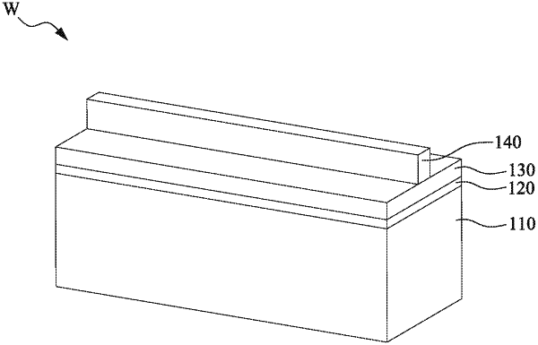
1. A method, comprising:
forming a semiconductor fin on a substrate;
forming a dielectric layer over the semiconductor fin;
forming a metal gate electrode in the dielectric layer and extending across the semiconductor fin;
forming a source/drain regions on the semiconductor fin and on opposite sides of the metal gate electrode;
performing a first non-zero bias plasma etching process to the metal gate electrode; and
after performing the first non-zero bias plasma etching process, performing a first zero bias plasma etching process to the metal gate electrode.