| CPC H01L 29/513 (2013.01) [H01L 29/1608 (2013.01); H01L 29/401 (2013.01); H01L 29/7803 (2013.01); H01L 29/7813 (2013.01); H01L 29/517 (2013.01)] | 23 Claims |
|
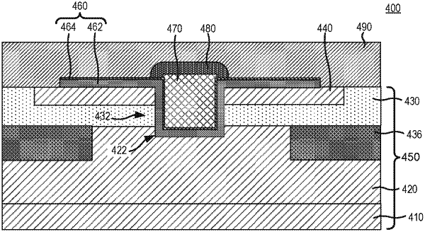
1. A semiconductor device, comprising:
a semiconductor layer structure that comprises silicon carbide, the semiconductor layer structure comprising a source region and a trench formed in the semiconductor layer structure, where at least some corners of the trench are rounded;
a gate dielectric layer on a top surface of the source region and within the trench, the gate dielectric layer comprising lower corners and upper corners, where at least one of the lower corners and upper corners comprises a rounded corner;
a gate electrode on the gate dielectric layer opposite the semiconductor layer structure; and
a dielectric isolation pattern on the gate electrode and the gate dielectric layer,
wherein the gate dielectric layer extends laterally beyond sidewalls of the gate electrode and sidewalls of the dielectric isolation pattern.
|