| CPC H01L 29/4991 (2013.01) [H01L 21/28088 (2013.01); H01L 29/6653 (2013.01); H01L 29/66545 (2013.01); H01L 29/6656 (2013.01); H01L 29/66795 (2013.01); H01L 21/0206 (2013.01); H01L 21/02164 (2013.01); H01L 21/0217 (2013.01); H01L 21/02236 (2013.01); H01L 21/02255 (2013.01); H01L 21/02271 (2013.01); H01L 21/02274 (2013.01); H01L 21/0274 (2013.01); H01L 21/0332 (2013.01); H01L 21/0337 (2013.01); H01L 21/31053 (2013.01); H01L 21/31111 (2013.01); H01L 21/3212 (2013.01); H01L 21/76224 (2013.01); H01L 29/4966 (2013.01)] | 20 Claims |
|
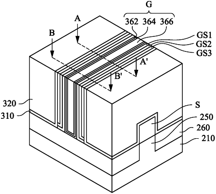
1. A device, comprising:
a semiconductive fin having source and drain regions and a channel region between the source and drain regions;
an isolation dielectric layer surrounding a bottom of the semiconductive fin;
a gate feature over the channel region of the semiconductive fin;
a first spacer around the gate feature;
source and drain features respectively in the source and drain regions of the semiconductive fin;
a gate oxide layer extending from one of the source and drain features, through beneath the gate feature, to another one of the source and drain features;
an interlayer dielectric layer around the first spacer; and
a void between the first spacer and the interlayer dielectric layer and spaced apart from the gate feature and the source and drain features, wherein the void is directly above the gate oxide layer and has:
a first air gap portion directly above the semiconductive fin;
a second air gap portion directly above the isolation dielectric layer, wherein the first air gap portion and the second air gap portion have different heights; and
a contact etch stop layer between the first spacer and the interlayer dielectric layer, wherein a top surface of the contact etch stop layer is lower than a top surface of the interlayer dielectric layer.
|